King’s working visit to MESA+ Nanolab University of Twente

- by maurya18@gmail.com
- December 19, 2024

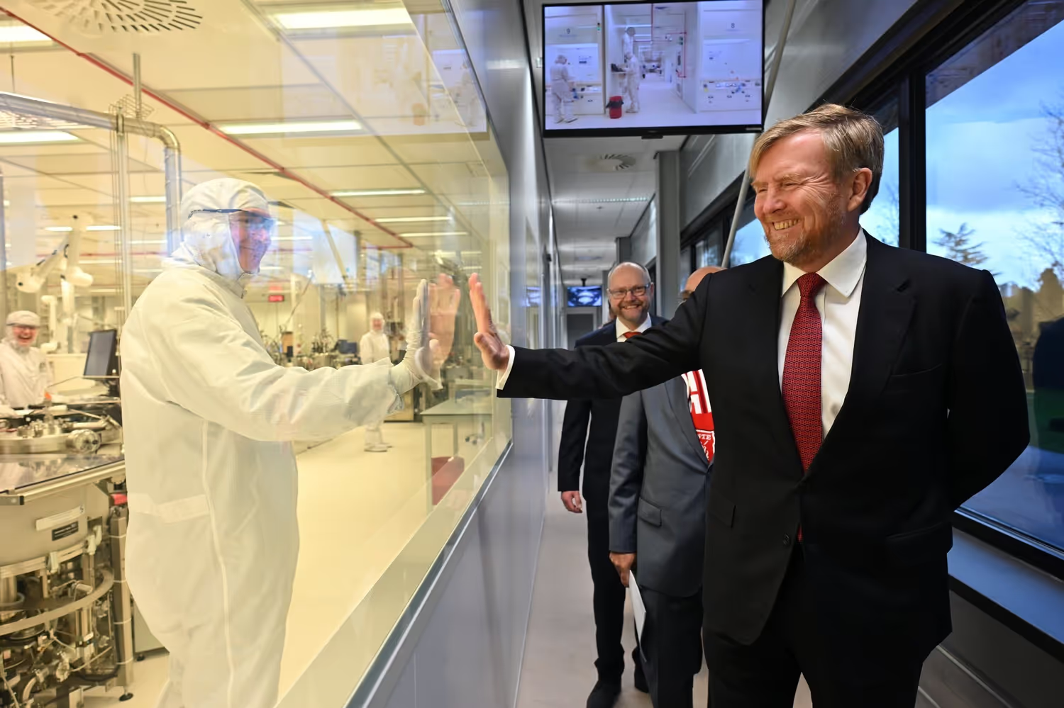
His Majesty the King paid a working visit to the University of Twente’s MESA+ NanoLab in Enschede today. The visit was all about integrated photonics, from idea through research to product.
The King was received by Vinod Subramaniam, the President of the University of Twente’s executive board, and the scientific and business directors of MESA+ Hans Hilgenkamp and Timo Meinders.
The King was given a tour of the MESA+ NanoLab and the Cleanroom was followed by an explanation of current developments and an explanation of the role of the cleanroom in integrated photonics. The King then spoke with students from the ROC van Twente, Saxion University of Applied Sciences and the UT.
Saxion student Julia Hennink spoke with the King about the Beethoven project aimed at the development of the chip industry. She discussed the different levels of education and the cooperation between them. Julia: “All links are important, but the roles of HBO and especially MBO are undervalued in this, despite the important contribution in the industry.”
Olympic highlights at the nanoscale
UT PhD student Femke Witmans talked about the ‘Nanolympics’: a project with the aim of giving nanotechnology a face and making it visible for the Netherlands. “Nanotechnology plays a big role in our society, but often remains invisible, which is why we decided to combine this with the power and energy of the Olympic Games. I thought it was extra special that we were able to let our King, as a fanatical supporter of TeamNL, relive several Olympic highlights, but on the nanoscale. It shows how impressive and versatile nanotechnology is and I hope that the King experienced this as well.”
From research to product
Twente is developing unique technology for mirrors that ASML uses in their EUV machines. Intensive academic research takes place here, in close collaboration with the business community. At the XUV Lab, a fascinating explanation of the research into EUV mirrors followed and the crucial importance of Twente research for products was emphasized.
“Twente is one of the world leaders in the field of Silicon Nitride Technology and Quantum Photonics and the emerging and promising platform Aluminium Oxide, both in terms of research and business. The triple helix is well developed so that all the ingredients are present regionally to bring fundamental research to the market. We have built up a good track record in the region and the King’s visit to see this with our own eyes was a wonderful recognition of our regional strength”, says Timo Meinders, Managing Director, MESA+ Institute.
Finally, a short tour took place at spin-off companies QuiX Quantum and LioniX in the innovation center The Gallery to talk about (quantum) photonics. The working visit ended with a roundtable discussion about the developments, opportunities and challenges for the Twente region in the field of photonics and chip technology. And about academic research in collaboration with the business community.
Round table discussion
The statements of this conversation were about the collaboration between education, research and business, among other things. It was discussed that ASML can only grow if Twente grows. Twente companies such as Demcon and VDL-ETG are indispensable for the growth of the large Dutch chip tech companies. The discussion partners went in search of the preconditions.
All kinds of wonderful studies were looked at today. The discussion was about how we can convert this research into activity in integrated photonics. There was unanimous agreement that cooperation between the knowledge institutions, government and business is the key to success in Twente.
“I look back with great satisfaction on the visit of His Majesty the King. It is a recognition of the strength of Twente’s ecosystem for photonics and chip technology, and the strength of cooperation in the region, with other knowledge institutions, government, and the business community. Twente is indispensable for the growth ambitions of the Netherlands in chip technology, and those collaborations play a very important role in this,” concludes Vinod Subramaniam.
Photonics
Photonics is a scientific discipline that focuses on technology based on light (photons). In integrated photonics, light is guided into materials on a chip. This forms the basis for new sensor concepts for medical applications, for example, and for ultra-fast, energy-efficient information technology.
The Latest News
-
January 1, 2025Hardloopkalender 2025: onze favoriete loopjes van komend jaar
-
January 1, 2025Trailrun kalender 2025: deze trails zijn in Nederland de moeite waard
-
January 1, 2025Netherlands | Locations | Baker McKenzie
-
December 30, 2024PGGM stapt in datacenters van Penta Infra – M&A
-
December 30, 2024Knot vindt dat belastingstelsel aan ingrijpende hervorming toe is


